原子力基盤技術データベースのメインページへ
作成: 1999/09/27 大島 武
データ番号 :170017
単色陽電子ビームを用いた炭化ケイ素(SiC)半導体のイオン注入層の欠陥評価
目的 : SiC電子素子作製のための不純物導入技術の開発
研究実施機関名 :日本原子力研究所高崎研究所技術開発課、筑波大学物理工学系谷川研究室
応用分野 :材料工学、半導体工学
概要 :
SiC半導体は耐環境性素子への応用が期待されており、不純物導入技術の確立が実用化の課題となっている。SiCにおいてはイオン注入法を用いた不純物導入が有望であるが、発生する照射欠陥が注入層の電気特性を低下させるため、照射欠陥の振舞いを明らかにすることが重要となっている。単色陽電子ビームを用いることで注入層内の空孔型欠陥の振舞いを調べることができ、注入及び注入後熱処理の最適化を図ることが可能となる。
詳細説明 :
SiCは耐環境性素子への応用が期待されているが、素子化に不可欠である不純物導入技術が確立されていない。SiCはドナーやアクセプタ不純物の熱拡散係数が非常に小さく熱拡散法が適用できないことから、イオン注入による不純物導入が有望視されている。しかし、イオン注入法には非熱平衡的に不純物を添加できる利点があるのと同時に、多量の照射欠陥が導入されるため、注入不純物の電気的活性化には照射欠陥を除去し注入層の結晶性を回復させる必要がある。SiCでは注入により発生する照射欠陥の構造やアニール挙動に関する情報が少なく、注入条件・注入後熱処理条件の最適化には至っていない。このため、SiCへのイオン注入技術の確立には欠陥の除去を正確に把握することが不可欠である。
陽電子消滅は空孔型欠陥の検出に非常に有効な測定手段である。単色陽電子ビームを用いることで試料中に入射する陽電子深さを制御することができ、低速陽電子ビームを用いることでイオン注入層といった表面から数百ナノメートル領域の欠陥評価が可能である。そこで、我々は低速単色陽電子ビームを用いてイオン注入SiCの欠陥評価を行った。
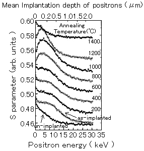
図1 Annealing temperature dependence of the S-E curve for the 6H-SiC implanted with 1x10¹³ P+/cm2 at RT. Typical S-E curves for annealed samples are shown in the figure. The mean implantation depth of positrons is shown in the upper horizontal axis. The solid lines represent the fitting results of the S-E curves. The S values are shifted by the relation S(E)+7x10⁻³Ta, where Ta is annealing temperature, between RT and 1000 ℃ and above1200 ℃, S(E)+7.005x10⁻³Ta-5.5x10⁻³.(原論文1より引用。 Reproduced from Applied Physics 1998; A 67, 407-412, Fig.1(p.409), T.Ohshima*, A.Uedono**, K.Abe*, H.Itoh*, Y.Aoki*, M.Yoshikawa*, S.Tanigawa**, and I.Nashiyama*, Characterization of vacancy-type defects and phosphorus donors introduced in 6H-SiC by ion implantation, Copyright(1998), with permission from Springer-Verlag. )
図1に、室温で燐イオンを1x10¹³/cm2注入した六方晶SiCのS値と入射陽電子エネルギーの関係の熱処理による変化を示す。図には比較のため未注入試料の結果も示している。S値は陽電子の消滅により発生するガンマ線(511keV)のドップラー広がりの大きさに関係したパラメータであり、この値より空孔型欠陥に関する情報を得ることができる。未注入試料において15keV以下のエネルギーでS値が上昇しているが、これは入射した陽電子の外方拡散と表面での消滅に関係する。注入後は20keV以下のエネルギー領域でS値が未注入試料に比べ増大する。これは注入により発生した空孔型欠陥に陽電子が捕獲されることに起因する。図中の実線は、各深さでのS値をパラメータとして陽電子の拡散方程式を解くことで求めたフィッティングラインである。
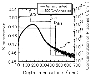
図2 Depth profiles of S parameter in implanted 6H-SiC. The solid and broken lines represent the results obtained for as-implanted and 800 ℃-annealed samples, respectively. For reference, the depth profile of P atoms determined from secondary ion mass spectroscopy for 6H-SiC implanted at RT with 200keV P+ 1x10¹⁵ /cm2 at RT is also shown.(原論文1より引用。 Reproduced from Applied Physics 1998; A 67, 407-412, Fig.1(p.409), T.Ohshima*, A.Uedono**, K.Abe*, H.Itoh*, Y.Aoki*, M.Yoshikawa*, S.Tanigawa**, and I.Nashiyama*, Characterization of vacancy-type defects and phosphorus donors introduced in 6H-SiC by ion implantation, Copyright(1998), with permission from Springer-Verlag. )
図2にフィッティングにより決定されたS値と深さの関係を示す。例として注入直後(実線)、800℃熱処理後(点線)の試料より得られた結果を示した。注入直後の試料では欠陥層と無欠陥層の2層で解析でき(境界をDd/f、欠陥層のS値をS1と記述)、S1の値から注入後に残留する空孔型欠陥の大きさがシリコン空孔(VSi)と炭素空孔(VC)の複合体(複空孔VSiVC)と同程度であることが分かった。一方、800℃熱処理後は欠陥層中にS値の異なる2層が存在するという結果が得られた(欠陥層間の境界をD1/2、表面側の欠陥層のS値をS1、深い側をS2と記述)。
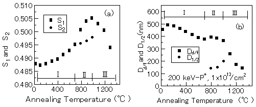
図3 a: Annealing-temperature dependence of estimated S parameter for the 6H-SiC implanted at 1x10¹³ P+/cm2 at RT. The S1, closed squares, and S2, closed circles, represent the S parameters in the first and the second blocks, respectively. b: Annealing-temperature dependence of the position of the interface of each block, D. The closed squares and circles represent Dd/f and D1/2, respectively.(原論文1より引用。 Reproduced from Applied Physics 1998; A 67, 407-412, Fig.1(p.409), T.Ohshima*, A.Uedono**, K.Abe*, H.Itoh*, Y.Aoki*, M.Yoshikawa*, S.Tanigawa**, and I.Nashiyama*, Characterization of vacancy-type defects and phosphorus donors introduced in 6H-SiC by ion implantation, Copyright(1998), with permission from Springer-Verlag. )
熱処理によるS 及びDd/fの変化を図3(a), (b)に示す。領域I(各温度領域は図中に記載)におけるS 、Dd/fの変化は、VSiやVCの移動による深部からの結晶性回復と、それらが他の空孔型欠陥と結合することによる空孔型欠陥の大きさの増大で解釈できる。領域IIはVSiVC等の複空孔が空孔型欠陥に結合して、さらにサイズの大きい空孔クラスターが形成されることで解釈できる。領域IIIでは空孔クラスターの消滅とその結果生ずる深部からの結晶性の回復がみられ、1400℃の熱処理後には欠陥層が完全に消滅するという結果が得られた。
注入層の電気特性を調べたところ、キャリア濃度及び移動度が1200℃以上の熱処理により急激に増加し、1400℃以上の熱処理で飽和することが分かった。これは、領域IIIでみられた結晶性の回復とともに注入層の電気特性が向上していることを示している。また、注入温度や注入量と熱処理による欠陥層回復との関係についても陽電子を用いて評価を行っており、高温注入を行うことで熱処理時に引き起こされる空孔型欠陥のクラスター化が抑制され電気特性が向上することを明らかにしている。
コメント :
低速の単色用電子ビームを用いることで、数百ナノメートルといった非常に薄い層の空孔型欠陥に関する情報を非破壊で得ることが可能となる。イオン注入層の結晶性の改善は半導体材料(SiCに限らず)の素子特性向上のために必要不可欠であり、低速の単色陽電子ビームが非常に有効な手段となる。
原論文1 Data source 1:
Characterization of vacancy-type defects and phosphorus donors introduced in 6H-SiC by ion implantation
T. Ohshima*, A. Uedono**, K. Abe*, H. Itoh*, Y. Aoki*, M. Yoshikawa*, S. Tanigawa**, I. Nashiyama*
Japan Atomic Energy Research Institute, ** Institute of Materials Science, University of Tsukuba
Applied Physics A 67, pp.407-412 (1998).
原論文2 Data source 2:
Investigation of vacancy-type defects in P+-implanted 6H-SiC using monoenergetic positron beams
A. Uedono*, T. Ohshima**, H. Itoh**, R. Suzuki***, T. Ohdaira***, S. Tanigawa*, Y. Aoki**, M. Yoshikawa**, I. Nashiyama**, T. Mikado***
Institute of Materials Science, University of Tsukuba, **Japan Atomic Energy Research Institute, *** Electrotechnical Laboratory
Japanese Journal of Applied Physics 37, pp.2422-2429 (1998).
原論文3 Data source 3:
Characterization of residual defects in cubic silicon carbide subjected to hot-implantation and subsequent annealing
H. Itoh*, T. Ohshima*, Y. Aoki*, K. Abe*, M. Yoshikawa*, I. Nashiyama*, H. Okumura**, S. Yoshida**, A. Uedono***, S. Tanigawa***
Japan Atomic Energy Research Insitute, ** Electrotechnical Laboratory, *** Institute of Materials Science, University of Tsukuba
Journal of Applied Physics 82, pp.5339-5347 (1997).
参考資料1 Reference 1:
イオン注入及び注入後熱処理した3C-SiC中の残留欠陥の研究
大島 武*, 伊藤 久義*, 上殿 明良**, 鈴木 良一***, 石田 夕起***, 高橋 徹夫***, 吉川 正人*, 児島 一聡*, 大平 俊行***, 梨山 勇*, 谷川 庄一郎**, 奥村 元***, 吉田 貞史***, 三角智 久***, 岡田 漱平*
*日本原子力研究所、**筑波大学物質工学系、***電子技術総合研究所
電子技術総合研究所彙報 vol.62, pp31-38 (1998).
キーワード:単色陽電子ビーム(monoenergetic positron beam), 炭化ケイ素(silicon carbide), イオン注入(ion implantation), 空孔型欠陥(vacancy-type defects), 注入後熱処理(post-implantation annealing)
分類コード:170303
原子力基盤技術データベースのメインページへ